
Applied Materials opens $5 billion chip research hub to accelerate semiconductor innovation
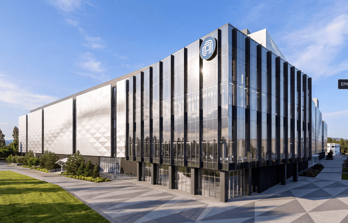
Applied Materials Inc. has unveiled the Equipment and Process Innovation and Commercialization (EPIC) Center, a $5 billion facility in Silicon Valley designed to accelerate semiconductor innovation through industry-wide collaboration. The facility aims to reduce chip development cycles by at least 30% and foster breakthroughs in AI and advanced computing.

Editor, Lazyfounder
30 SEC SUMMARY
- Applied Materials Inc. has opened a $5 billion chip research facility, the EPIC Center, in Silicon Valley to accelerate semiconductor innovation.
- The 600,000-square-foot facility includes nearly four acres of cleanroom space for collaborative R&D.
- Founding partners include TSMC, Intel, Samsung, Micron, and SK hynix, with a focus on 3D architectures, advanced packaging, and energy-efficient computing.
- The EPIC Center aims to reduce chip development cycles by at least 30% through industry-wide collaboration.
- Industry leaders emphasize the need for collaboration to address a multitrillion-dollar opportunity in AI computing.
TABLE OF CONTENTS
KEY HIGHLIGHTS
- Applied Materials Inc. has launched the Equipment and Process Innovation and Commercialization (EPIC) Center, a $5 billion chip research facility in Silicon Valley.
- The EPIC Center spans 600,000 square feet and includes nearly four acres of cleanroom space for semiconductor R&D.
- Founding partners include TSMC, Intel, Samsung, Micron, SK hynix, Broadcom, and Advantest, along with academic institutions like Stanford University and UC Berkeley.
- The facility will focus on 3D architectures, advanced packaging, low-resistance wiring, and hybrid bonding to accelerate chip innovation.
- Applied Materials CEO Gary Dickerson estimates the EPIC Center could reduce new chip development lifecycles by at least 30%.
Applied Materials launches $5 billion chip research facility
Applied Materials Inc. has opened the Equipment and Process Innovation and Commercialization (EPIC) Center, a $5 billion semiconductor research facility in Silicon Valley. According to SiliconANGLE, the facility is designed to accelerate collaborative innovation in chipmaking by providing a shared space for industry-wide research and development.
The EPIC Center spans more than 600,000 square feet and includes almost four acres of cleanroom space, making it one of the largest facilities of its kind. Its primary goal is to enable breakthroughs in semiconductor manufacturing technologies through joint projects among leading chipmakers and equipment providers.
Focus on collaborative R&D and industry partnerships
The EPIC Center will host engineers from Applied Materials alongside counterparts from founding partners, including TSMC, Intel Corp., Samsung Electronics, Micron Technology, and SK hynix. Additional partners, such as Broadcom, Advantest, and academic institutions like Stanford University, UC Berkeley, and UCLA, will also participate in collaborative projects.
The facility will prioritize innovations in 3D architectures, advanced packaging techniques, low-resistance wiring, and hybrid bonding. These areas are critical for advancing chip performance, energy efficiency, and integration, particularly for AI and high-performance computing applications.
Reducing development cycles and industry impact
Applied Materials CEO Gary Dickerson stated that the EPIC Center could compress the development lifecycle of new chip technologies by at least 30%. This acceleration is expected to benefit industries ranging from healthcare and industrial production to education and consumer electronics.
Intel CEO Lip-Bu Tan emphasized the importance of collaboration in capitalizing on a multitrillion-dollar opportunity in AI computing. He highlighted the need for joint efforts in areas like transistors, interconnects, and advanced packaging to drive the next wave of semiconductor innovation.
What this means
Lazyfounder analysis — our interpretation, not reported fact.
The opening of the EPIC Center marks a significant shift in how semiconductor innovation is approached. For decades, chipmakers and equipment providers have largely pursued R&D in isolation, protecting their intellectual property while shouldering the high costs of cutting-edge facilities. The EPIC Center’s collaborative model could democratize access to advanced infrastructure, allowing smaller players and startups to participate in high-stakes innovation without prohibitive investment.
For founders and operators in the broader tech ecosystem, this facility is a signal of where the industry is headed: faster iteration, shared risks, and cross-pollination of ideas. If successful, the EPIC Center could serve as a template for other industries where R&D costs are skyrocketing, such as biotech or quantum computing. However, the real test will be whether competitors can set aside short-term rivalries to create long-term value—a challenge that has derailed similar initiatives in the past.
Key takeaways
- For founders in semiconductor and AI infrastructure, the EPIC Center represents a rare opportunity to collaborate with industry leaders on cutting-edge R&D without bearing the full cost of a private facility.
- Startups in adjacent sectors, such as AI hardware or energy-efficient computing, should monitor breakthroughs from the EPIC Center, as they could unlock new product roadmaps or partnerships.
- The collaborative model of the EPIC Center signals a shift in the semiconductor industry toward shared innovation, which may inspire similar R&D consortia in other sectors.
- Operators should note the emphasis on reducing development cycles—a 30% acceleration could redefine competitive timelines for chip-dependent products.
FAQ
Why is the EPIC Center significant for the semiconductor industry?
The EPIC Center is significant because it provides a shared R&D facility for major chipmakers and equipment providers to collaborate on next-generation technologies. This model aims to reduce development costs, accelerate innovation cycles, and foster breakthroughs in areas like 3D architectures and advanced packaging, which are critical for AI and high-performance computing.
Who are the founding partners of the EPIC Center?
The founding partners of the EPIC Center include TSMC, Intel Corp., Samsung Electronics, Micron Technology, and SK hynix. Additional partners include Broadcom, Advantest, and academic institutions like Stanford University, UC Berkeley, and UCLA.
How could the EPIC Center impact startups and smaller companies?
The EPIC Center could lower barriers to entry for startups and smaller companies by providing access to advanced semiconductor R&D infrastructure and expertise. This could enable them to participate in innovation that would otherwise be cost-prohibitive, potentially accelerating product development and time-to-market.
Related on Lazyfounder
Sources
- SiliconANGLE · 2026-10-13
Applied Materials opens new $5B chip research facility to accelerate collaborative semiconductor innovation
This story is an original summary drafted with AI by Lazyfounder from the reporting listed above and checked by automated validation. Facts are attributed to their original publishers; sections marked as analysis are Lazyfounder's. Where a source is in another language, facts were machine-translated and quotations are reported, not reproduced. Read the original coverage via the links, and see our AI policy and corrections policy.

About the author
Editor, Lazyfounder
Tarun Mottlia edits LazyFounders, covering Indian startups, funding rounds, AI and product launches. Every story on the site is AI-assisted and checked against its cited sources before publication.
More stories by Tarun MottliaGet the LazyFounder Brief
Startup, funding and AI news in a five-minute read. Join the early-access list.